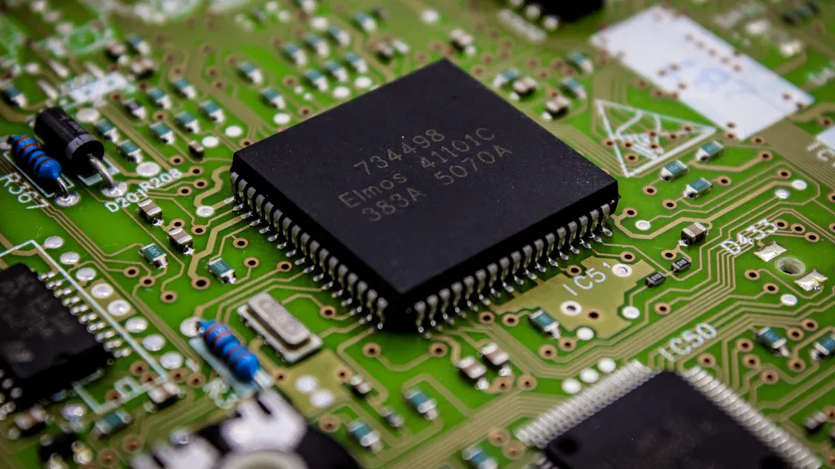
When you work with double-sided PCB boards, you can use an auto router to speed up your design process. This tool helps you connect components on both sides of the board. You get better routing options and can reduce manual errors. Careful setup and review help you avoid problems later. Always check the results and make manual changes to ensure your circuit works well.
Double-Sided PCB Boards and Auto Router Essentials
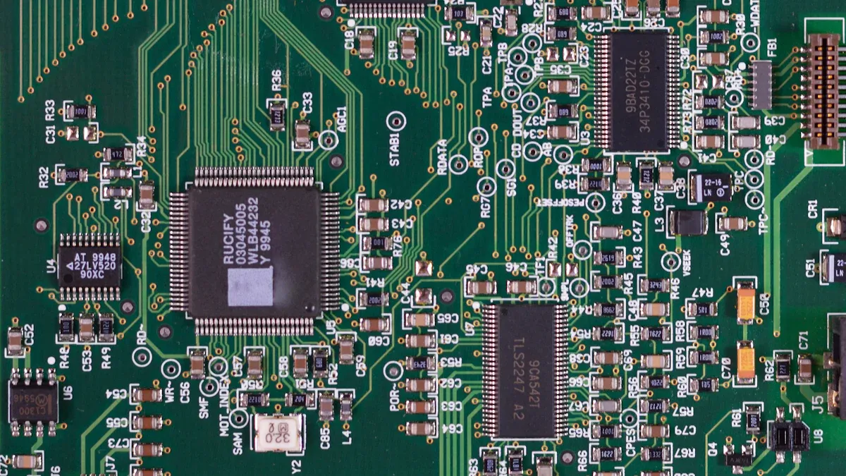
Routing Flexibility with Two Layers
You gain more options when you design with double-sided PCB boards. You can route signals on both the top and bottom layers. This flexibility helps you create compact and complex circuits. The table below shows how double-sided boards compare to single-sided boards:
| Característica | Single-Sided PCB | Double-Sided PCB |
|---|---|---|
| Conductive Layers | One layer only | Two layers (top and bottom) |
| Routing Options | Limited, can complicate designs | More intricate routing possible |
| Component Density | Lower, due to space constraints | Higher, allows for compact designs |
| Use of Vias | Not applicable | Yes, enables connections between layers |
Puede ver que double-sided boards allow for greater routing flexibility and higher component density. You can use vias to connect traces between layers. This feature lets you design more advanced circuits without raising costs too much.
Managing Layers and Vias in Auto Router
When you use an auto router for double-sided boards, you can control how the tool places vias. Some auto routers, like the Situs Topological Autorouter, use smart mapping to find the best paths for your traces. You can adjust a slider to set the number of vias. If you move the slider to the right, the auto router uses fewer vias but takes longer to finish. If you move it to the left, the tool works faster but adds more vias. You can guide the auto router to balance speed and via count for your design.
- You can reduce via usage for better signal quality.
- You can allow more vias for faster routing in less critical areas.
Unique Challenges in Double-Sided Auto Routing
You face new challenges when you route double-sided boards. You must manage more connections and higher component density. The auto router helps you handle complex designs quickly. You still need to review the results and make manual tweaks. You must check for overcrowded traces and make sure critical signals have clear paths. Double-sided routing gives you more freedom, but you need to watch for signal integrity and manufacturing limits.
| Ventajas | Descripción |
|---|---|
| Greater routing flexibility | Allows for more complex and compact designs than single-layer PCBs. |
| Moderate increase in complexity | Enables the design of more intricate circuits without excessive cost. |
| Balance between cost and performance | Provides a cost-effective solution while enhancing performance. |
| Improved density | Increases circuit density without a significant rise in costs. |
Tip: Always review your auto router results and adjust critical paths by hand for best performance.
Step-by-Step Guide to Using Auto Router for Double-Sided Boards
Preparing the PCB Layout for Auto Router
Before you start using the auto router, you need to prepare your PCB layout carefully. Good preparation helps you avoid problems and makes the routing process smoother. Follow these steps to get your board ready:
- Run a design rule check (DRC) to catch any errors in your layout.
- Review the Routing Setup Report and make sure it does not show any design rule violations.
- Check all errors, warnings, and hints. These messages help you spot potential issues that could confuse the auto router.
- Fix any routing-related rule violations. This step improves the performance of the auto router and helps you get better results.
- Set up your design rules to match the technology and requirements of your board.
Consejo: Always resolve errors before you run the auto router. This step saves you time and prevents routing failures later.
Setting Design Rules for Double-Sided Routing
You need to set the right design rules for successful double-sided auto routing. These rules help you avoid problems like short circuits, signal loss, or manufacturing errors. Here are some important design rules to consider:
- Trace Width: Use online calculators to pick the right trace width. Ask your fabrication house about their minimum trace width.
- Minimum Spacing: Keep at least 6 mils between traces for low-voltage designs. Use more space for higher voltages to prevent crosstalk or arcing.
- Optimize Trace Lengths: Keep important signal traces as short as possible. Shorter traces reduce delays and signal loss, especially in high-speed circuits.
- Avoid Sharp Corners: Use 45-degree angles or curves instead of sharp corners. This practice helps prevent signal reflection and makes manufacturing easier.
- Layer Stackup and Via Usage: Try to use fewer vias and place them carefully. Too many vias can make your board complex and increase thermal stress.
- Thermal Management: Use wider traces for paths that carry a lot of current. This step helps manage heat and keeps your board safe.
- Design for Manufacturability (DFM): Make sure your design matches what your fabrication house can build. This step helps you avoid production problems.
Nota: Setting clear and realistic design rules helps the auto router work better and gives you a board that is easier to manufacture.
Configuring Auto Router for Two-Layer Operation
When you set up the auto router for a double-sided board, you need to adjust several settings. These settings help the tool route traces efficiently on both layers and meet your design needs. Focus on these key configuration options:
- Clearance Constraints: Define special clearance rules for components with closely spaced pads. This step prevents shorts and makes soldering easier.
- Routing Via Style: Set up a Routing Via Style rule for all nets. Adjust the style if some nets need different via sizes or types.
- Routing Layers: Create a Routing Layers rule and enable both the top and bottom layers for routing. This setting tells the auto router to use both sides of the board.
- Layer Directions: Choose preferred routing directions for each layer. For example, you can set the top layer to route horizontally and the bottom layer to route vertically. This approach helps the auto router organize traces and avoid congestion.
Consejo: Double-check your auto router settings before you start. A well-configured tool saves you time and reduces the need for manual fixes.
Running the Auto Router and Reviewing Results
You have set up your double-sided PCB and configured all the rules. Now you can run the auto router. This tool works quickly and connects the traces on both layers. You watch as the software places traces, adds vias, and tries to solve every connection.
After the auto router finishes, you need to review the results. This step helps you find problems and improve your design. You look at several important metrics. These indicators show how well the routing process worked.
| Metric/Indicator | Descripción |
|---|---|
| Routing grid | Shows the distance between grid lines for conductor placement. Lower values can help the auto router fit more traces, but may crowd the board. |
| Obstacle closeness | Measures how close traces get to obstacles like pads. Lower values allow tighter routing, but traces may get too close to pads. |
| Trace bend | Counts the number of bends in traces. More bends can make routing easier, but may complicate signal flow. |
| Layer change | Tracks the number of vias. More vias mean more layer changes, which can make manufacturing harder. |
| 45 deg trace | Shows the number of 45-degree trace segments. More segments can help routing, but may increase complexity. |
You check these metrics to see if the auto router made good choices. If you see too many vias, you may want to adjust your settings and try again. If traces get too close to pads, you risk short circuits. You look for traces with many bends, because sharp turns can weaken signals.
Consejo: Always use the review step to catch problems early. You can fix issues before you send your board for manufacturing.
You also scan the board visually. You look for crowded areas, long traces, and places where signals might cross. You check if the power and ground traces are wide enough. You make sure the auto router did not miss any connections.
If you find problems, you can run the auto router again with new settings. You can also fix traces by hand. Careful review helps you build a reliable PCB.
Manual Optimization After Auto Router
Adjusting Critical Signal Paths
After you finish with the auto router, you need to check your critical signal paths. These paths carry important signals, like clocks or high-speed data. If you want your board to work well, you must make sure these signals travel safely and without interference.
- Separate noisy nets, such as clocks, from quiet nets, like data lines. This helps prevent unwanted noise.
- Plan how power moves across your board. Focus on the Power Distribution Network to keep signals stable.
- Place bypass and decoupling capacitors close to chips. These parts help filter out noise.
- Minimize the use of vias in critical signal paths. Too many vias can cause signal problems.
- Keep trace widths constant for high-speed signals. This helps maintain signal quality.
- Use differential pairs and control trace lengths to reduce timing issues.
- Run signal integrity checks. Look for impedance mismatches, crosstalk, and timing errors.
Consejo: Manual routing is crucial for enhancing the effectiveness of automated routing tools in PCB design.
Minimizing Unnecessary Vias
Too many vias can make your board harder to build and may hurt performance. You can take several steps to reduce unnecessary vias:
- Merge similar components, such as capacitors or resistors, to simplify the layout.
- Use SMD (Surface Mount Device) components. These parts do not need vias and save space.
- Try blind or buried vias if your manufacturer supports them. These vias use less surface area.
- Arrange components in a compact way. This reduces gaps and crossovers, so you need fewer vias.
- Plan your routing to avoid unnecessary trace crossings and layer changes.
- Talk with your manufacturer. They can tell you the best way to avoid extra vias.
Note: Fewer vias mean better signal integrity and easier manufacturing.
Enhancing Power and Ground Connections
Strong power and ground connections keep your board stable. You can improve these connections with a few simple steps:
- Use separate ground planes for high and low-voltage areas. This reduces crosstalk and keeps signals clean.
- Make sure ground planes are solid and do not have splits. This lowers voltage drops.
- Add stitching capacitors when signals change ground reference. Use ground fill to keep the ground uniform.
- Apply multi-point grounding. This keeps ground voltage steady and reduces loops.
- Use wide ground traces for high-current paths. This prevents overheating.
- Place bypass and decoupling capacitors near chips. These help stop ground bounce and coupling.
Remember: Good power and ground design helps your board run smoothly and reliably.
Troubleshooting and Avoiding Common Auto Router Pitfalls
Addressing Overcrowded or Inefficient Routing
You may notice that your PCB layout looks crowded or messy after auto routing. Overcrowded routing can cause errors and make your board hard to manufacture. You can spot these problems by looking for too many vias, tangled traces, or parts placed too close together.
| Problema | Solución |
|---|---|
| Overly complex routing | Simplify your routing and remove unnecessary vias. This step reduces errors and speeds up production. |
| Poor via placement | Place microvias carefully in high-density areas. Good via design lowers costs and avoids delays. |
You can also improve your layout by moving parts to better positions. Inefficient part placement often leads to noise, signal problems, and heat issues. Try to group related components together. This makes routing easier and keeps your board neat.
Tip: Always review your layout for crowded areas before sending your design to production.
Preventing Crosstalk and Signal Integrity Issues
Crosstalk happens when signals interfere with each other. You can prevent this by following a few simple rules:
- Use ground planes to shield sensitive signals from noise.
- Keep enough space between traces. Try to space traces at least three times their width apart.
- Route high-speed and sensitive traces at right angles across layers.
- Avoid sharp angles in your traces. Use smooth curves or 45-degree bends.
- Place digital signals over a ground plane to lower crosstalk.
- Use differential pairs for signals that need extra protection.
Increasing the distance between signals, especially outside tight spots, helps reduce unwanted interference. Good spacing and careful routing keep your signals clean and strong.
Balancing Layers and Manufacturing Considerations
You need to balance your use of both layers to get the best results. If you put too many traces on one layer, you may run into problems with heat or signal quality. Spread your traces evenly between the top and bottom layers.
Think about how your design will be built. Too many vias or complex routing can slow down manufacturing and raise costs. Work with your manufacturer to understand their limits. Choose via sizes and trace widths that match their process.
Note: A balanced and simple design is easier to build and works more reliably. Always check your layout with your manufacturer’s guidelines before finalizing your board.
Best Practices and Recommended Auto Router Tools
Tips for Effective Double-Sided Auto Routing
You can improve your double-sided PCB design by following expert tips. Start by using ground planes to boost signal integrity. Place components in a way that makes routing easier. Use decoupling capacitors to keep power lines stable and reduce noise. Guard traces help shield sensitive signals and lower crosstalk. Keep power traces wide and away from important signal paths. Route traces with care to minimize noise and avoid sharp turns. Controlled impedance guidelines help you with high-speed designs. Modern ECAD tools offer features that make routing more efficient.
Tip: Leverage built-in ECAD features and analog route mapping to solve complex routing challenges.
Recommended Auto Router Tools Including HUASIFEI
You have many choices when picking an auto router tool for double-sided PCB boards. Each tool offers unique features to help you design better circuits. The table below shows some popular options:
| Tool | Características principales |
|---|---|
| Altium Designer | ActiveRoute for guided routing, 3D visualization, high-quality CAD tools, auto-interactive routing, design rule compliance. |
| ExpressPCB Plus | Powerful auto-router, extensive component library, 3D visualization, DRC for error-free designs. |
| KiCad EDA | Open-source, active community, cross-platform compatibility, design rule check (DRC) functionality. |
| HUASIFEI | Efficient auto routing, user-friendly interface, supports double-sided PCB design, reliable performance. |
Altium Designer gives you advanced routing accuracy and a unified design environment. ExpressPCB Plus offers auto-routing and a large component library. KiCad EDA is open-source and works on many platforms. HUASIFEI provides efficient auto routing and supports double-sided boards with a simple interface.
Verifying and Validating the Final PCB Design
You need to check your PCB design before sending it to manufacturing. Follow these steps to make sure your board works well:
- Run a design rule check to catch layout errors.
- Optimize your design for manufacturability.
- Verify that all components work and are available.
- Check signal integrity, thermal performance, and mechanical fit.
- Review Gerber and drill files for accuracy.
- Inspect for assembly defects like bridging or tombstoning.
You should also set up DRC parameters, run checks during design, and perform a final DRC check after placing all components. A DFM check helps you avoid manufacturing problems. Your contract manufacturer will test the board during production. Final PCBA testing ensures the board is strong and works as expected.
Note: Careful validation helps you avoid costly mistakes and ensures your double-sided PCB meets all requirements.
You can achieve efficient double-sided PCB designs by following key steps:
- Avoid routing across splits or crowded zones.
- Keep transmission lines on a single layer when possible.
- Use ground transfer vias for layer changes.
- Set up trace lengths and differential pairs with constraint managers.
Manual review helps you catch crosstalk and signal integrity issues that auto routers might miss. Try different auto router settings and tools to find what works best for your project. Auto routers save time, but your careful checks ensure a reliable board.
PREGUNTAS FRECUENTES
What is an auto router tool in PCB design?
An auto router tool helps you connect traces between components on your PCB. You set rules, and the tool finds paths for signals. This saves you time and reduces manual errors.
Can you use auto routers for high-speed signal routing?
You can use auto routers for basic routing. For high-speed signals, you should route critical paths by hand. Manual routing gives you better control over signal integrity.
Tip: Always check high-speed traces after auto routing.
How do you reduce the number of vias in your design?
You place components close together and plan your layout. You use SMD parts when possible. Fewer vias make your board easier to build and improve signal quality.
- Place related components together
- Use SMD parts
What should you check after auto routing your PCB?
You review trace widths, via count, and spacing. You run a design rule check. You look for crowded areas and make sure power and ground traces are wide enough.
| Checkpoint | Por qué es importante |
|---|---|
| Trace width | Prevents overheating |
| Via count | Eases manufacturing |
| Spacing | Avoids short circuits |