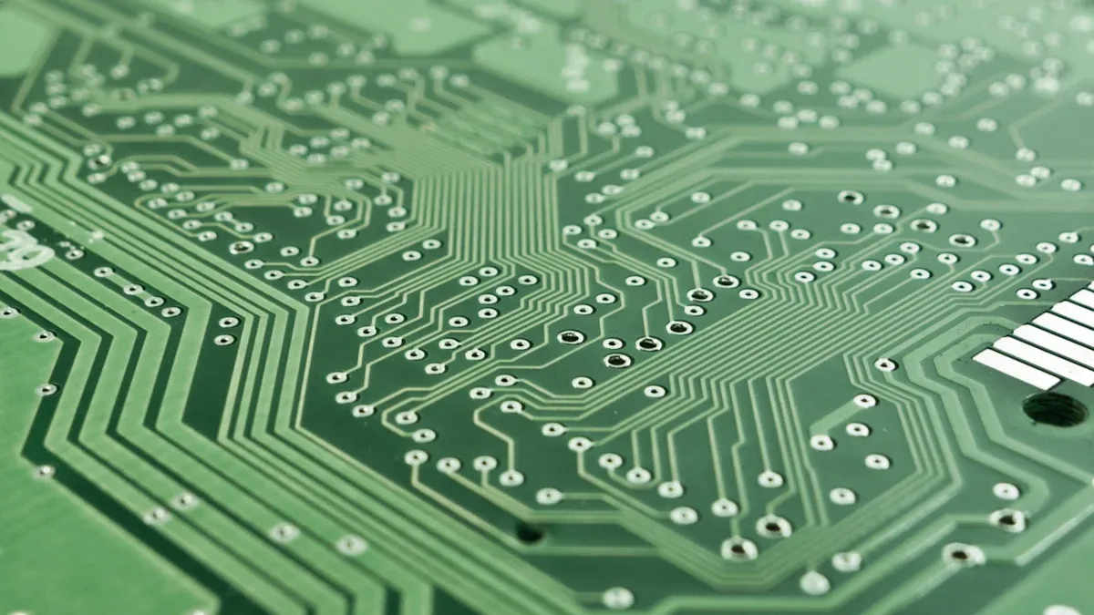
You can make your pcb design faster and more reliable by using an auto router. With automatic routing, you save time and reduce errors in your pcb layout. Many routing tool features support creativity and combine manual and automated routing for better efficiency.
- You gain improved quality by reducing manual mistakes.
- Automated placement helps optimize your circuit board.
HUASIFEI sets a high standard for innovation and quality, inspiring you to use the best design practices.
Auto Router Setup
PCB Design Preparation
You start your circuit board design by capturing the schematic and assigning footprints to each component. This step ensures that every part has a physical representation on your pcb. Next, you prepare your design for automatic routing by following these steps:
- Place components in optimal positions. Keep high-speed nets separate from noisy ones.
- Set routing priorities. Begin with power nets, then move to critical signals like oscillators or high-speed interfaces, and finish with quiet nets.
- Configure your layers in the Layer Stack Manager. This setup helps the automated routing tool work efficiently.
Grouping related components improves design efficiency. You can use module definition files to organize components. Select Placement Edit under Application Mode, choose your components, and save the module definition file. Apply this file to group components automatically. After creating your schematic, import the netlist into your layout. Route components in one room, then use the copy room format option to apply changes across all rooms. This process helps you manage complex pcb layouts and supports high-quality results.
HUASIFEI’s focus on quality and innovation shows the value of careful preparation. When you take time to organize your design, you set the stage for a successful auto router experience.
Defining Design Rules
Before you use an automated routing tool, you must define clear design rules. These rules guide the routing tool and help prevent errors. The table below shows some critical rules:
| Design Rule Type | Beschreibung |
|---|---|
| Routing Width Rules | Set the minimum width for traces to carry the required current. |
| Clearance Constraints | Specify the minimum distance between traces and other objects to avoid short circuits. |
| High-Speed Design Considerations | Address special needs for routing high-speed signals to keep signal integrity. |
You should also follow minimum width and spacing guidelines for traces. Optimize trace paths for signal integrity. Consider manufacturing constraints, such as material limits and fabrication tolerances. These steps ensure your circuit board design meets both quality and safety standards.
Selecting Auto Router Tools
Choosing the right automated routing tool is important for your pcb project. Look for tools that give you control over routing paths. Some tools, like ActiveRoute, let you guide the routing for better results. Make sure the tool follows your design rules, including trace and pad clearances and impedance tolerances. Integration in a unified environment, such as Altium Designer, improves workflow and helps you catch errors early.
Auto-routing tools work best for less critical signals. For high-speed signals, use differential routing strategies to reduce noise and signal skew. Avoid sharp corners in signal routing to prevent signal reflections. By selecting the right tools and strategies, you improve the efficiency and quality of your automated trace routing.
Automatic Routing Process
Running the Auto Router
You can start the automatic routing process after you finish placing all components on your pcb. This step uses the auto router to connect the nets based on your design rules. Follow these steps to run the routing tool effectively:
- Open your layout file with all components placed.
- Go to the tools menu and select the routing tool, such as FreeRouting, to begin the process.
- Set your design rules and constraints. These rules help the auto router follow your requirements for trace width, clearance, and signal routing.
- Place components efficiently to reduce routing complexity. Good placement makes automatic routing easier and improves the final result.
- Manually route critical signals before starting the auto router. These signals often need special attention for signal integrity.
- Use net classes to prioritize sensitive signals. This step helps the routing tool handle important connections with care.
- Start the auto router and let it generate the initial routing paths.
Modern auto routers use advanced algorithms like river routing and topological mapping. These algorithms help the routing tool create efficient paths, reduce the number of vias, and improve the quality of your pcb design. You can guide the routing tool interactively in some software, which lets you control the routing strategy and edit paths as needed.
Tipp: Always check your layers before running the auto router. Fewer layers can make routing more challenging, but good placement and clear rules help the tool work better.
Reviewing Results
After the automatic routing process finishes, you need to review the results carefully. The routing tool may not always produce perfect paths, so you must check the layout for issues. Here are some best practices for reviewing your pcb:
- Group components using net classes or component classes. This helps you identify which areas need more attention.
- Use Rooms to organize groups of components. Keeping related parts together makes the layout cleaner.
- Check the proximity of components in the pcb layout. Components that are too close can cause routing problems.
- Import components from schematic sheets in order. This step keeps your circuit board design organized and maintains circuit integrity.
You should also look for common routing errors. Sometimes, the auto router may route traces too close to the edge of the pcb or create paths that are not optimal. If you find unsatisfactory results, you can undo the routing and try different settings. Drawing out large rails on the board during cleanup helps maintain a clean and organized layout. This step is important for both the function and appearance of your pcb.
PCB Manual Adjustments
You often need to make manual adjustments after automatic routing. The complexity of your pcb increases with more components, which means the auto router may not handle every detail perfectly. Manual routing experience becomes valuable at this stage.
- You may need to adjust traces for high-frequency signals or heat-generating components. These parts require careful review to ensure signal integrity and proper heat dissipation.
- Check for traces that the auto router placed around the edges of the pcb. These paths can cause problems and may need correction.
- Clean up the layout by moving traces, adjusting via positions, and improving the overall routing flow.
Anmerkung: Automated trace routing saves time, but you must always review and refine the results. Manual adjustments help you achieve the highest quality for your circuit board.
By combining automatic routing with careful manual review, you ensure that your pcb design meets both functional and quality standards. This approach helps you create reliable and efficient designs, even as your projects become more complex.
Circuit Board Optimization
Layout Strategies
You can improve your pcb design by using smart layout strategies after automatic routing. The way you arrange components and select routing methods affects the efficiency and quality of your circuit board. Proper placement reduces signal interference and helps the routing tool create better paths. You should pay attention to the orientation of components and consider gate or pin swapping for easier routing. The table below shows common layout strategies that help optimize your pcb:
| Layout Strategy | Beschreibung |
|---|---|
| Area routers | Specify a section or layer for routing to control trace paths. |
| Single net routers | Route point-to-point connections for critical signals. |
| Bus routers | Group similar nets, such as memory data lines, for organized routing. |
| High-speed tuning routers | Match trace lengths for signals that need timing alignment. |
| Scribble routers | Sketch the desired path, letting the auto router finish the routing. |
| Batch routers | Route the entire pcb design in one step for efficiency. |
You can use these strategies to guide the routing tool and achieve a cleaner, more reliable pcb. HUASIFEI’s commitment to high standards inspires you to verify every step and strive for the best results in your circuit board design.
Fine-Tuning Settings
You can fine-tune settings in your auto router to get better automatic routing results. Adjusting these options helps you control routing density and signal routing paths. Here are some settings you should check:
- Routing width rules set how wide traces should be for different signals.
- Clearance constraints keep traces and pads at safe distances to prevent shorts.
- Routing via style matches track width and clearance for smooth connections.
- Component placement affects how easily the routing tool can connect nets.
- Keepouts define areas where routing should not occur, protecting sensitive parts.
- Avoid too many rules, which can slow down the routing tool and make processing harder.
- Set a width rule for all nets, and add special rules for critical signals or fine-pitch components.
You can adjust these settings to match your design needs and improve the outcome of automated trace routing.
Post-Routing Verification
After automatic routing, you need to verify your pcb to catch any errors and ensure quality. You should follow these steps for thorough post-routing checks:
- Setup DRC (Design Rule Check) with parameters for clearances, drill holes, and layers based on your circuit board manufacturer’s rules.
- Perform DRC checks during design changes to find violations early.
- Run a final DRC check after placing all components and finishing routing.
- Conduct a DFM (Design for Manufacturability) check to confirm your pcb can be produced without issues.
- Inspect the board during manufacturing with visual and optical tests.
- Test the finished circuit board for structural integrity and performance.
You can use these verification methods to ensure your pcb design meets high standards for quality and reliability. HUASIFEI’s dedication to excellence reminds you to always check your work and optimize every detail.
Avoiding Pitfalls in PCB Design
Common Auto Router Issues
You may notice several challenges when you use an auto router in your pcb design. Many designers find that automatic routing leaves some nets unconnected and creates paths that do not follow a clear strategy. This can make routing the remaining signals very difficult.
Because every time I use one, it leaves many nets unconnected, and the ones it does route are often poorly strategized (if there’s any strategy at all). This makes routing the remaining nets almost impossible.
You should also consider the limitations of routing tools. The table below highlights key concerns:
| Limitation Type | Beschreibung |
|---|---|
| Complexity Concerns | Advanced designs can overwhelm autorouters, requiring manual adjustments for optimal results. |
| Trade-offs | Relying solely on autorouters may yield suboptimal routing choices compared to experienced designers. |
| Over-automation | Excessive reliance on automation can hinder your ability to troubleshoot effectively. |
| Limited Intuition | Autorouters lack the contextual understanding that human designers possess, leading to poor decisions. |
| Potential for Increased Costs | Autorouters may introduce unnecessary components, raising production costs and affecting signal integrity. |
You may find that results are visually unappealing. Routing tools do not help with component placement, and changes to track widths or power planes can complicate the routing process. Learning to use automated trace routing effectively takes effort.
Tipps zur Fehlerbehebung
You can resolve many automatic routing problems by following a step-by-step approach. Here are some troubleshooting tips:
- Visual Inspection: Check for solder bridges, damaged traces, and correct component orientation.
- Test for Shorts and Open Circuits: Use a multimeter to identify shorts and open circuits.
- Verify Power Supply: Measure voltage and ensure proper power supply to the circuit board.
- Analyze Signal Integrity: Use an oscilloscope to check for signal issues in high-speed designs.
- Test Functionality Incrementally: Break down testing into smaller sections to isolate issues.
You should balance automatic routing with manual adjustments. Start by manually routing all critical nets, such as power lines and high-speed signals. Use the auto router for less critical signals. After the routing tool finishes, review and clean up the pcb. This hybrid approach helps you achieve better signal routing and overall design quality.
You can use both automatic and manual routing to optimize your pcb. Manual adjustments are essential for complex designs and critical signals. By combining these methods, you improve the reliability and performance of your layers and signals.
You can make your PCB design process faster and more reliable by using auto router tools. Auto-routing connects simple and complex nets while following design rules, as shown below:
| Mode | Beschreibung |
|---|---|
| Point-to-point Auto-routing | Connects simple nets quickly and accurately. |
| Batch Auto-routing | Routes miscellaneous nets using your rules. |
| Auto-interactive Routing | Lets you guide routing for complex designs. |
Combining auto-routing with manual review helps you meet performance goals. Always check and adjust traces for best results. HUASIFEI’s commitment to innovation inspires you to use these strategies for high-quality PCB projects.
FAQ
What is an auto router in PCB design?
An auto router is a tool that connects circuit paths on your PCB automatically. You set rules, and the tool creates the best routes for your signals. This saves you time and helps you avoid manual errors.
When should you use manual routing instead of auto routing?
You should use manual routing for high-speed signals, power lines, or sensitive analog paths. Manual routing gives you more control over trace length and placement. Auto routing works best for less critical connections.
How do you improve auto router results?
Place components carefully before running the auto router. Set clear design rules for trace width and spacing. Manually route important signals first. Review and adjust the auto-routed paths for better performance and reliability.
Can auto routers handle complex PCB designs?
Auto routers can help with complex designs, but you may need to make manual adjustments. For advanced boards, you should combine auto routing with manual review to ensure signal integrity and meet all design requirements.